
First revision of PCB complete
Working off the schematics from my last post, I started to complete PCB layout. The first task I took care of was establishing the board border and layout for connectors, since this defines where all the parts will have to go.
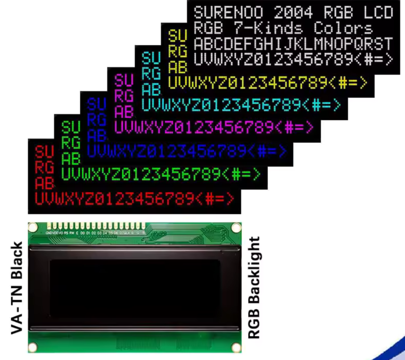
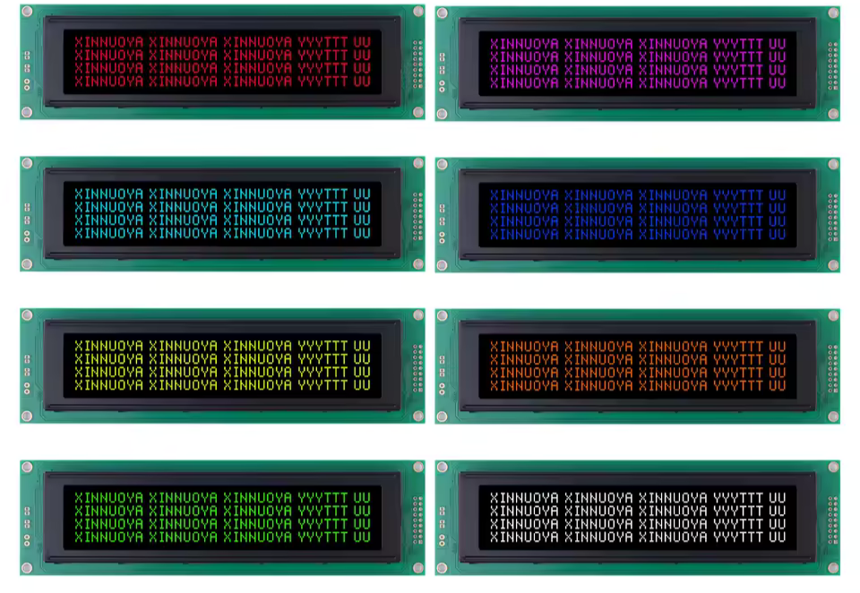
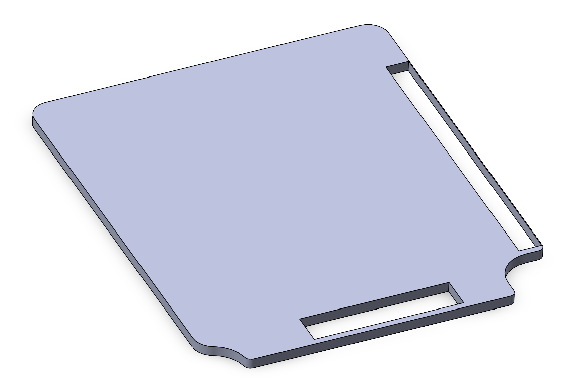
The board's size is restricted by the smallest sizes of LCDs that I want to use for the project, since I want those to be the limiting factors for enclosure size. The two smallest LCDs I've ordered for some prototyping are the standard 20x4 size LCDs in the T-Time MinuTe, and the T-Time W1 which has a 40x4 LCD with the same size characters.
With these guidelines in mind, I used the dimensions of both displays, plus their connector locations to create a simple outline of the PCB in SolidWorks.
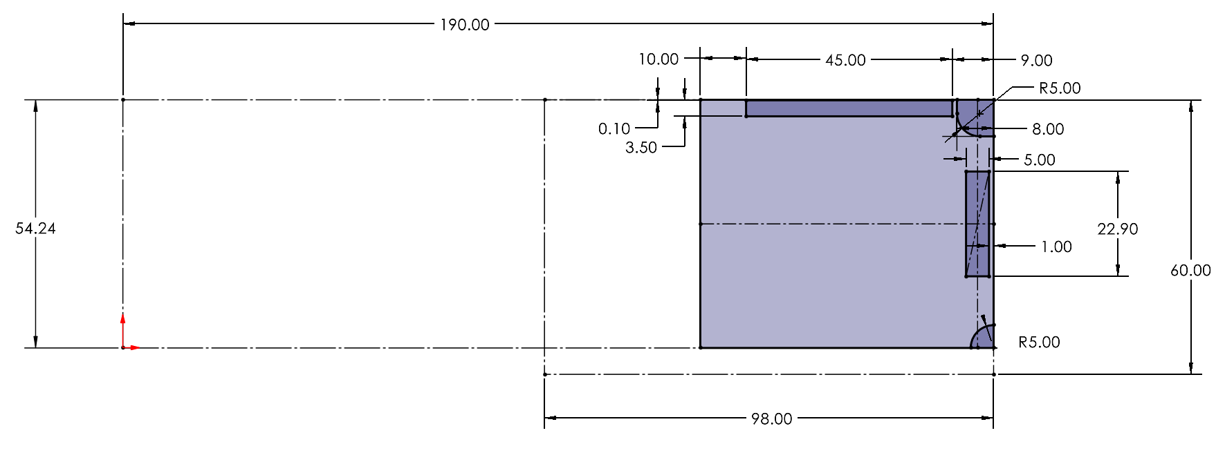
After this, I extruded the model, added some extra fillets and exported it as a DXF to import as a Edge Cut layer in KiCad.
It's rather difficult to summarize exactly how I planned the PCB layout, since it's more akin to art than engineering (aside from signal routing choices and trace sizing), but my workflow was somewhat similar to the schematic.
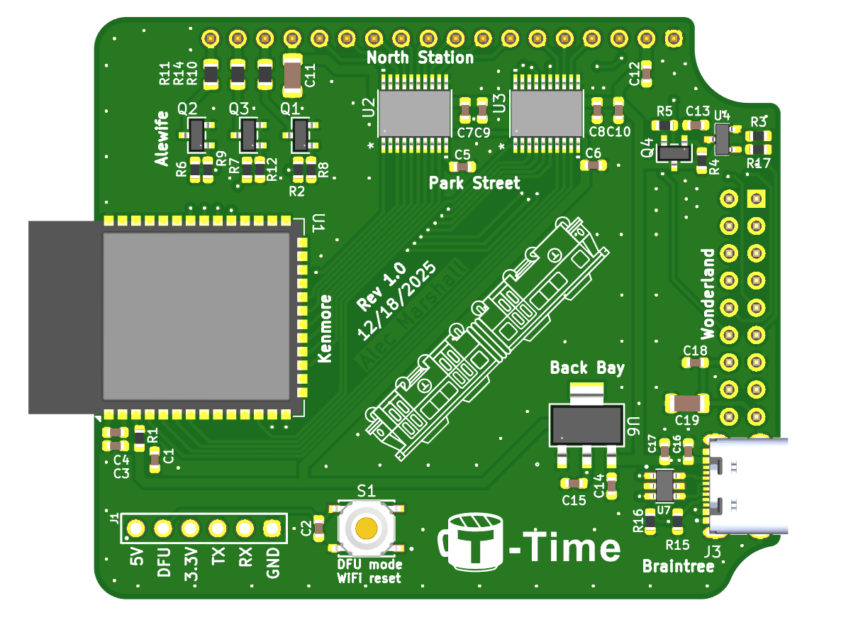
I first tackled placement of all the large items on the board like the ESP32, headers, and USB C port. These all have specific locations that are non-negotiable. The ESP has to be on the left side to allow the antenna room to stick out, the USB C port has to be on the right to allow the user to plug in the T-Time from the edge (top or bottom would be bad for desktop use), and the header positions are defined by the SolidWorks model and are inherently fixed.
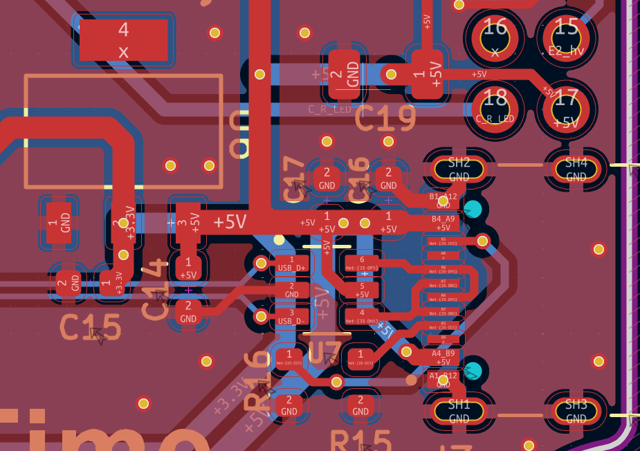
After those items were placed I went right to adding the USB-C input section, since that part of the design is fairly fixed as well. Also visible here is the 3.3V regulator which is just a 1117 series 800ma rated 3.3V LDO for powering the ESP32. Both sides of the board have GND pours, which provide the vast majority of ground connections for components. Another important tip for the design of the USB-C input is ensuring that the shield pins for the USB-C connector are attached to ground so that the shield functions effectively.
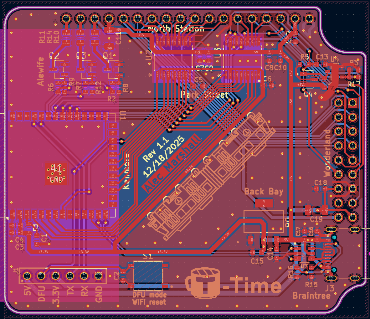
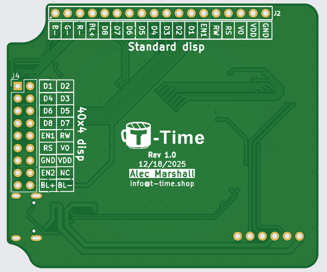
Since the front doesn't have room for it, I pushed the pinouts for the display headers to the back side of the board for anyone who might take the board out and use it for something else. It's also helpful to verify the connections while prototyping.
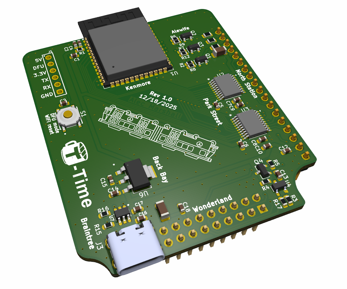
I also made this nice 3D render of the PCB using KiCad's built in raytracing engine! It's a good graphic for the T-Time website, and I really love that this is a native feature within KiCad.
0 Comments Add a Comment?