
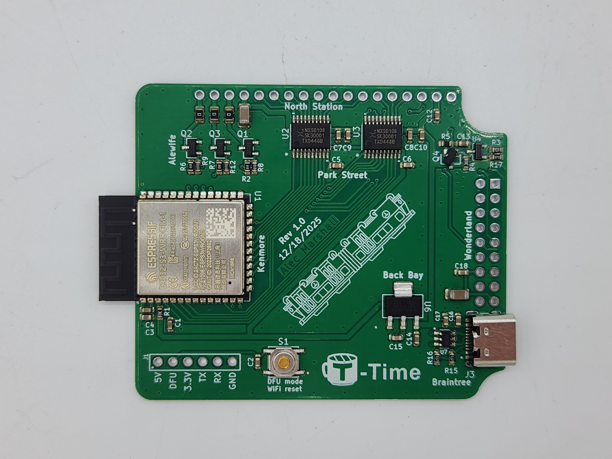
First revision of PCBs arrived
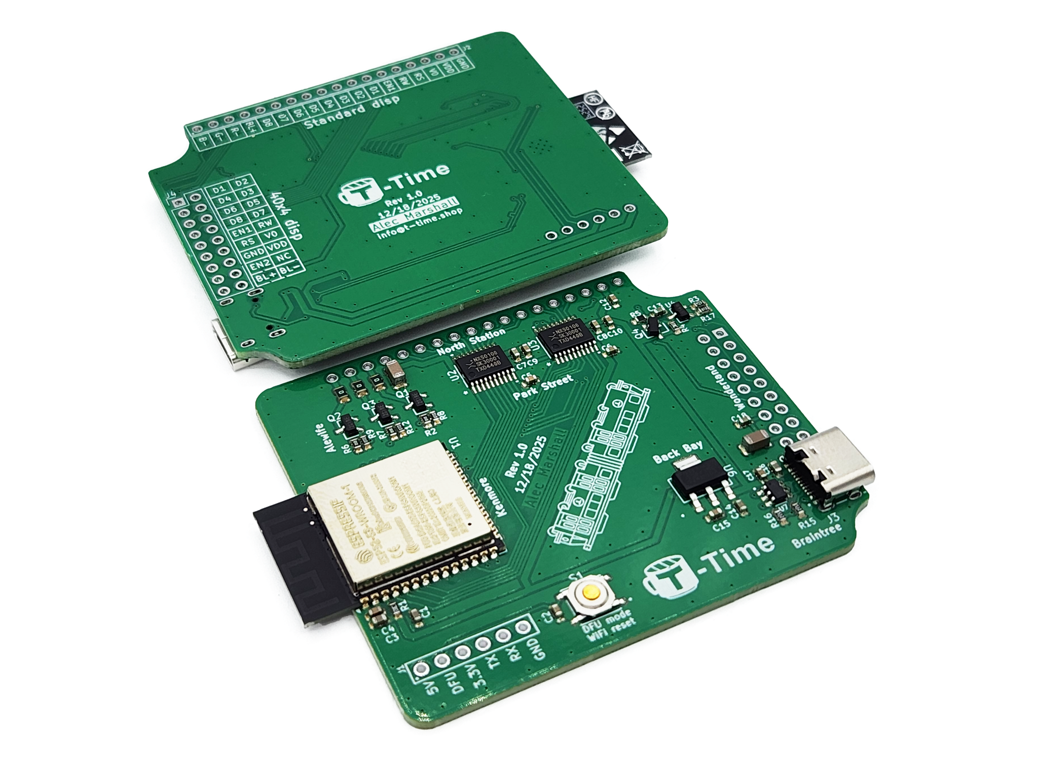
Finally, after a couple weeks of waiting, the PCBs arrived! My research lab has a large soldering room with a fancy board oven for SMD soldering, so I took a trip over there to begin the assembly.
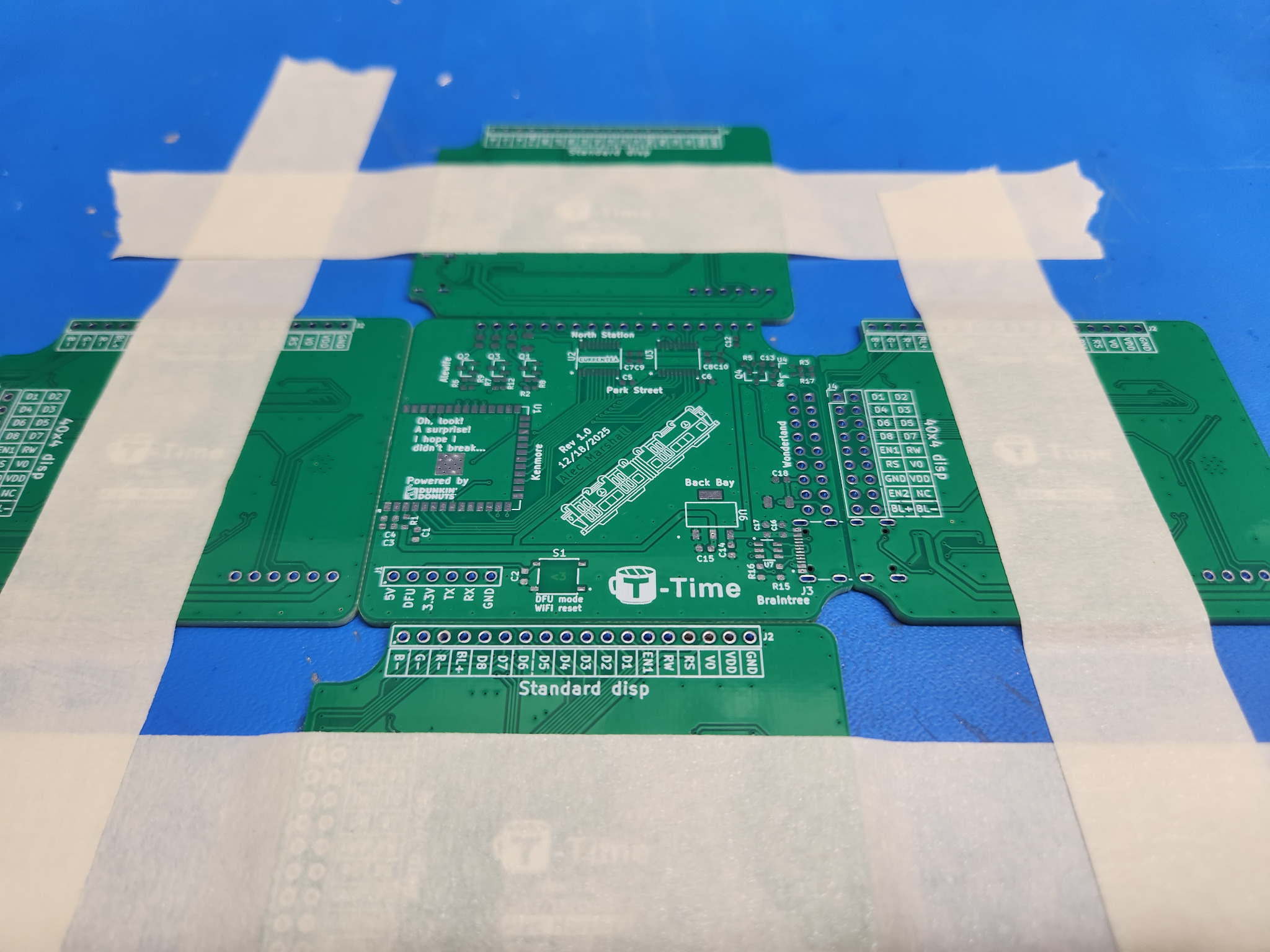
PCB Assembly:

Since I ordered a stencil with my PCBs, I prepared to spread solder paste across it by firmly holding one PCB in place using 4 others.
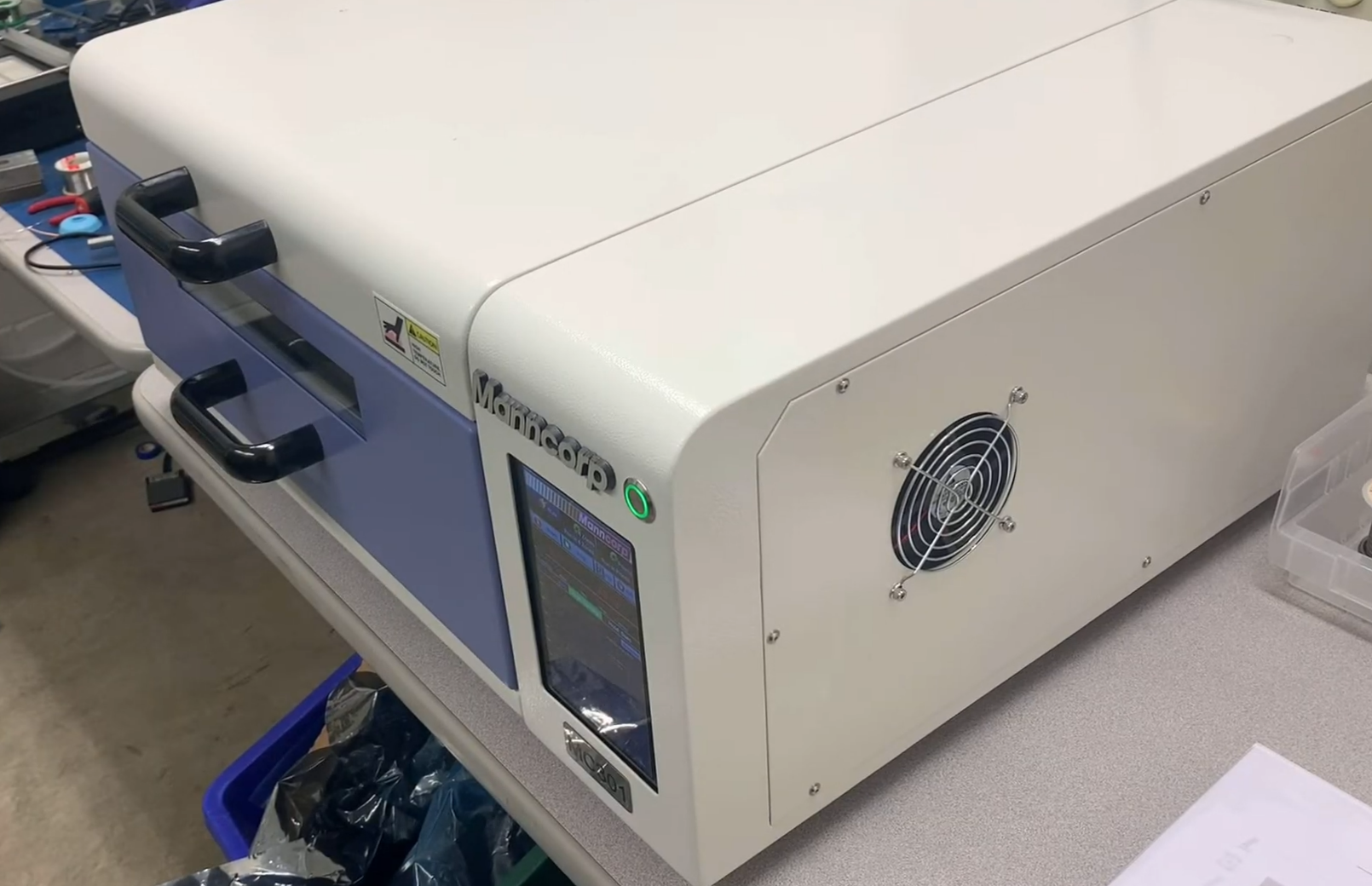
Finally, this board was ready for the board oven. If you're not familiar with them, it's basically just a large flat oven with precise surface temperature control. The oven automatically takes care of providing a "solder curve" which is the temperature profile that the solder manufacturer specifies for preheating, constant heating, reflowing, and cooling to provide the best solder joints possible.
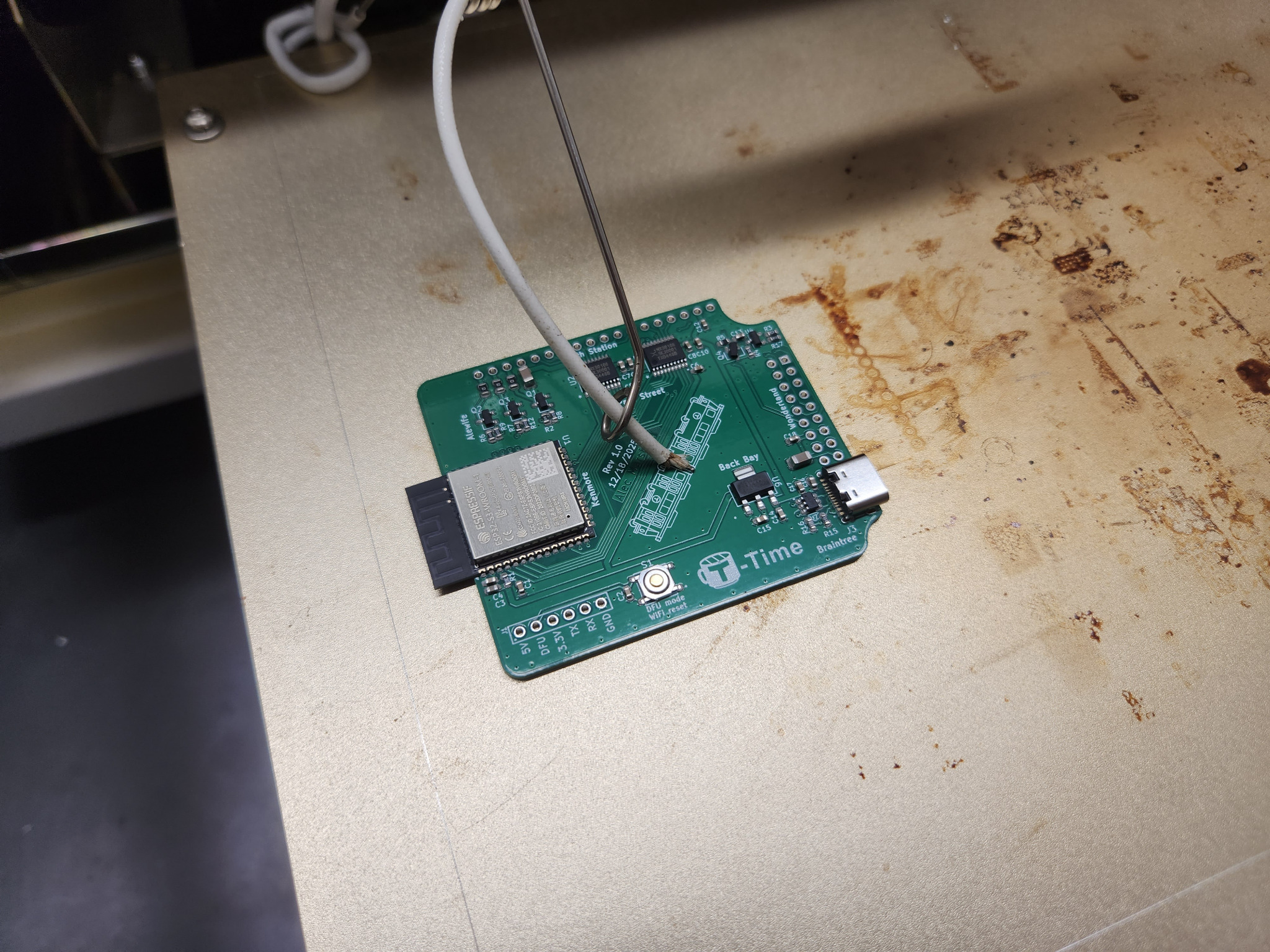
PCB testing results:
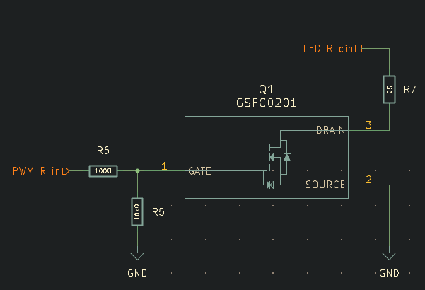
Although I'd love to say that the PCB worked perfectly first try, unfortunately there were a couple minor issues. The ESP32s worked perfectly, and all the power circuitry and LCD data lines had no issues. I ran into problems with the backlight MOSFETs and the contrast adjustment though.
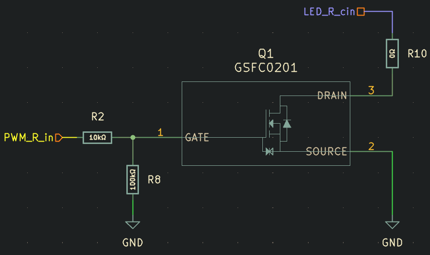
For the LED backlight MOSFETs, the issue was caused by the 5V level shifter's output glitching when used to drive the MOSFET gate. The level shifters I used are bidirectional (since the LCD can return data), and my best guess is that the high gate current from charging the MOSFET gate capacitance through a low value resistor was causing the bidirectional level shifter to feed back a low signal even when the ESP32's PWM signal was high.
I solved this by swapping the 10 ohm gate resistors for a 10kohm resistor, which although many orders of magnitude larger, appears to have done the trick while still adequately triggering the gates. I may investigate putting some sort of unidirectional push-pull level shifter between the gate and the microcontroller pin instead of the bidirectional logic level shifter to reduce switching loss.
The most major "mistake" of sorts on the board was the contrast control. Based on some digital contrast adjustment articles I'd read, I was under the impression that the "V0" pin on the LCD was a 0-5V "voltage supply" for the LCD module, where higher voltage meant higher contrast, however this is actually the exact opposite of the case. I designed my circuit to operate well near 5V, with a PWM controlled high side gate and RC filter, assuming it would be driving some sort of load, but since the V0 pin actually is intended to be adjusted near 0v (hence the name V0), it needs to be a very low voltage output instead.
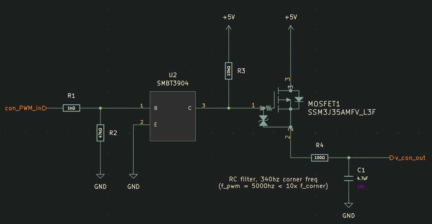
Although this circuit worked exactly as intended when tested with a load resistor, it makes complete sense that it would be worthless as a near ground return path for the LCD's drive circuitry. There is no path to ground for the current to flow through, and so the high side P-Channel MOSFET (unintentionally pictured as a N-Channel MOSFET) would charge C1 up to 5V, and nothing would happen. The LCD appeared to be totally off.
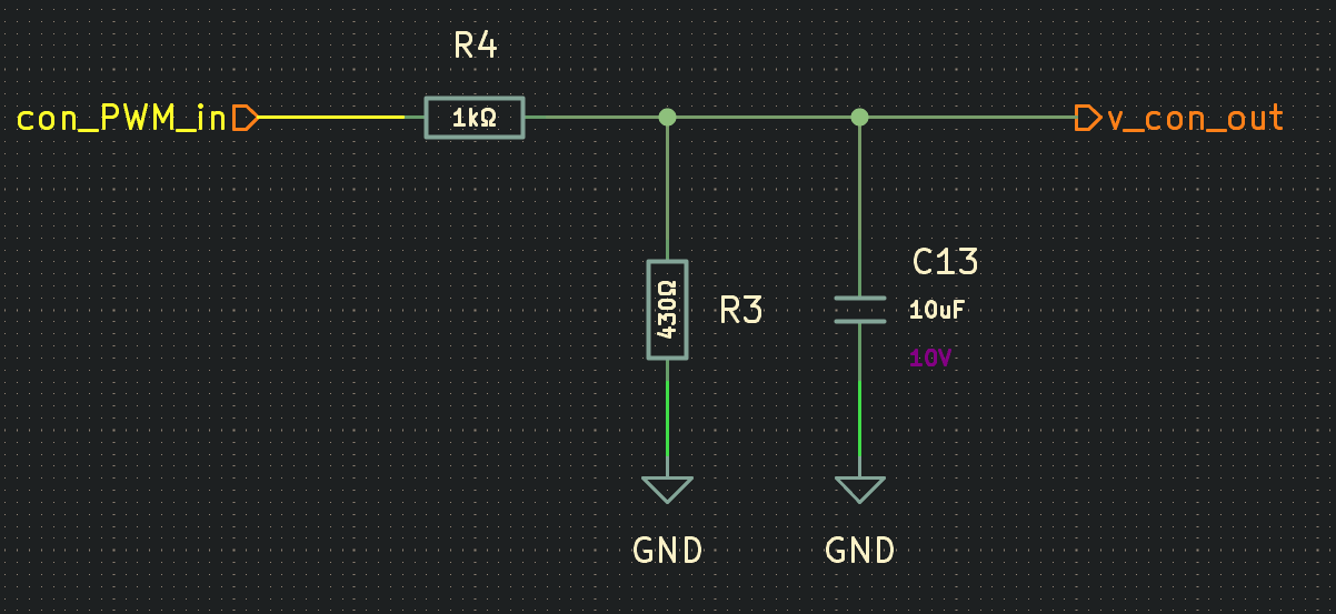
With this info in mind, the solution becomes remarkably easy. Since we want a lower voltage near-ground sink that only needs a couple milliamps of capability, I wired con_PWM_in directly to the ESP32's GPIO 38 pin, and formed a simple compound voltage divider and RC filter that drops the voltage down from 3.3V max to ~1.0V max. This is plenty of range for all the contrast adjustment circuits I tested. The 10uF cap also seemed to be plenty to smooth the signal for all of the LCDs I tested, even at very low voltages.
Sometimes the best solution is also the easiest and cheapest! Thankfully for this case, it was. I've also found a way to modify the prototype PCBs to still work (by scraping some soldermask, abusing old footprints, and replacing components). So I should still be able to produce some functional prototypes with the first revision of boards. I'll post more about those changes soon!
Looking forward to keep you guys updated on the project! I'm working more on case manufacturing and setting up the H2D for this week, but I'll spin a new revision of boards soon.
-Alec
0 Comments Add a Comment?